

Silkscreen
What is PCB Silkscreen?
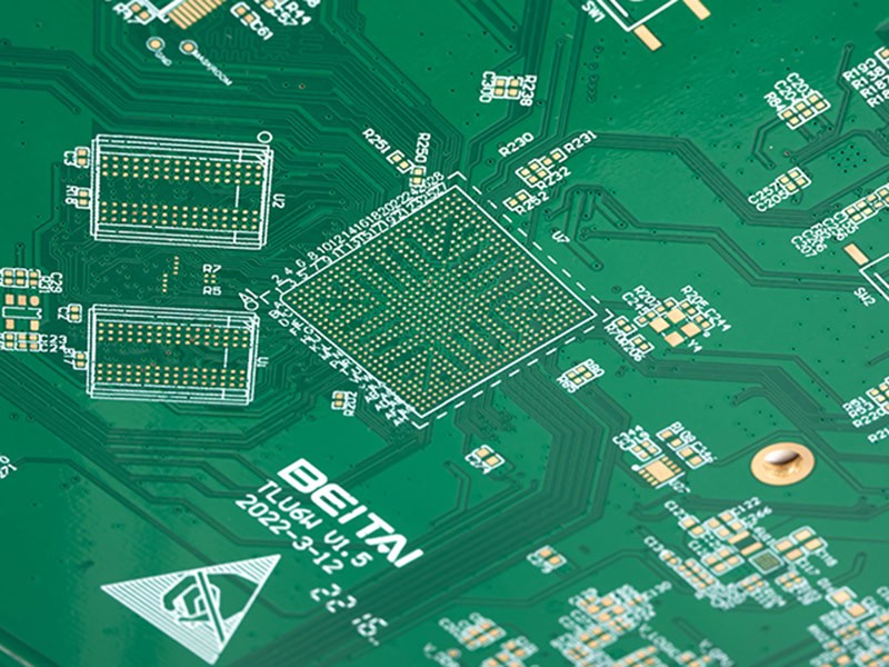
PCB silkscreen is a process where a layer of special non-conductive ink is applied to the surface of a printed circuit board (PCB) via screen printing. This layer is often used to identify component locations, test points, warning symbols, and other important information. Silkscreen is usually the last step in the PCB manufacturing process, ensuring clear and readable markings on the board to aid assembly and maintenance.
The main functions of PCB silk screen include:
01.
Identify components:
Provide component numbers and other important information to help technicians quickly identify them during assembly and repair.
02.
Provide reference
Display test points and connection information on the circuit board to ensure the accuracy of the assembly process.
03.
Warning signs
Mark safety warnings and instructions for use to prevent operating errors.
04.
Aesthetics
Improve the appearance quality of the PCB and make it more professional.
The production method of PCB screen printing mainly includes the following steps:
Make sure the PCB surface is clean and remove any dirt or grease so that the ink can adhere well.
Use PCB design software to create the screen pattern and generate the corresponding template.
Choose a special ink that is resistant to high temperature and chemical corrosion. Common colors are white, black and yellow.
-Place the prepared screen template on the PCB.
-Use a scraper to apply the ink evenly to the template and transfer the ink to the PCB surface through the screen.
Cure the ink by baking or UV irradiation to ensure that it is firmly attached to the PCB surface.
Finally, check whether the screen printing is clear and complete, and perform necessary functional tests to ensure that it meets the design requirements.
