1. DFM→2. Cut Material→3. Buried Via Drilling→4. Platting Copper→5. Inner Layer Dry Film→6. Inner Etching→7. Black Oxide →8. Laminating→9. PTH Drilling →10. Plated-through hole→11. Outer Dry Film→12. Pattern Plating→13. Outer Etching→14. Solders→15. Silk Screen→16. Surface Treatment→17. Routing→18. E-test→19. Final Visual Inspection(FQA、FQC)→20. Packing and Output
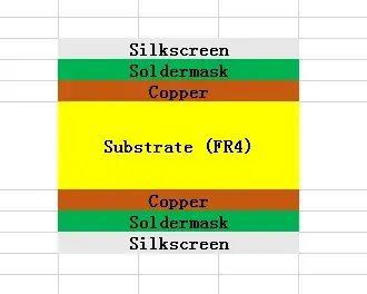
PCB can be single-sided (one copper layer), double-sided (two copper layers on both sides of one substrate layer), or multi-layer (outer and inner layers of copper, alternating with layers of substrate). Multi-layer PCB allow for much higher component density, because circuit traces on the inner layers would otherwise take up surface space between components. The rise in popularity of multi-layer PCB with more than two, and especially with more than four, copper planes was concurrent with the adoption of surface mount technology.
Substrate: The first, and most important, is the substrate, usually made of fiberglass. Fiberglass is used because it provides a core strength to the PCB and helps resist breakage. Think of the substrate as the PCB’s “skeleton”.
Copper Layer: Depending on the board type, this layer can either be copper foil or a full-on copper coating. Regardless of which approach is used, the point of the copper is still the same — to carry electrical signals to and from the PCB, much like your nervous system carries signals between your brain and your muscles.
Solder Mask: The third piece of the PCB is the solder mask, which is a layer of polymer that helps protect the copper so that it doesn’t short-circuit from coming into contact with the environment. In this way, the solder mask acts as the PCB’s “skin”.
Silkscreen: The final part of the circuit board is the silkscreen. The silkscreen is usually on the component side of the board used to show part numbers, logos, symbols switch settings, component reference and test points. The silkscreen can also be known as legend or nomenclature.
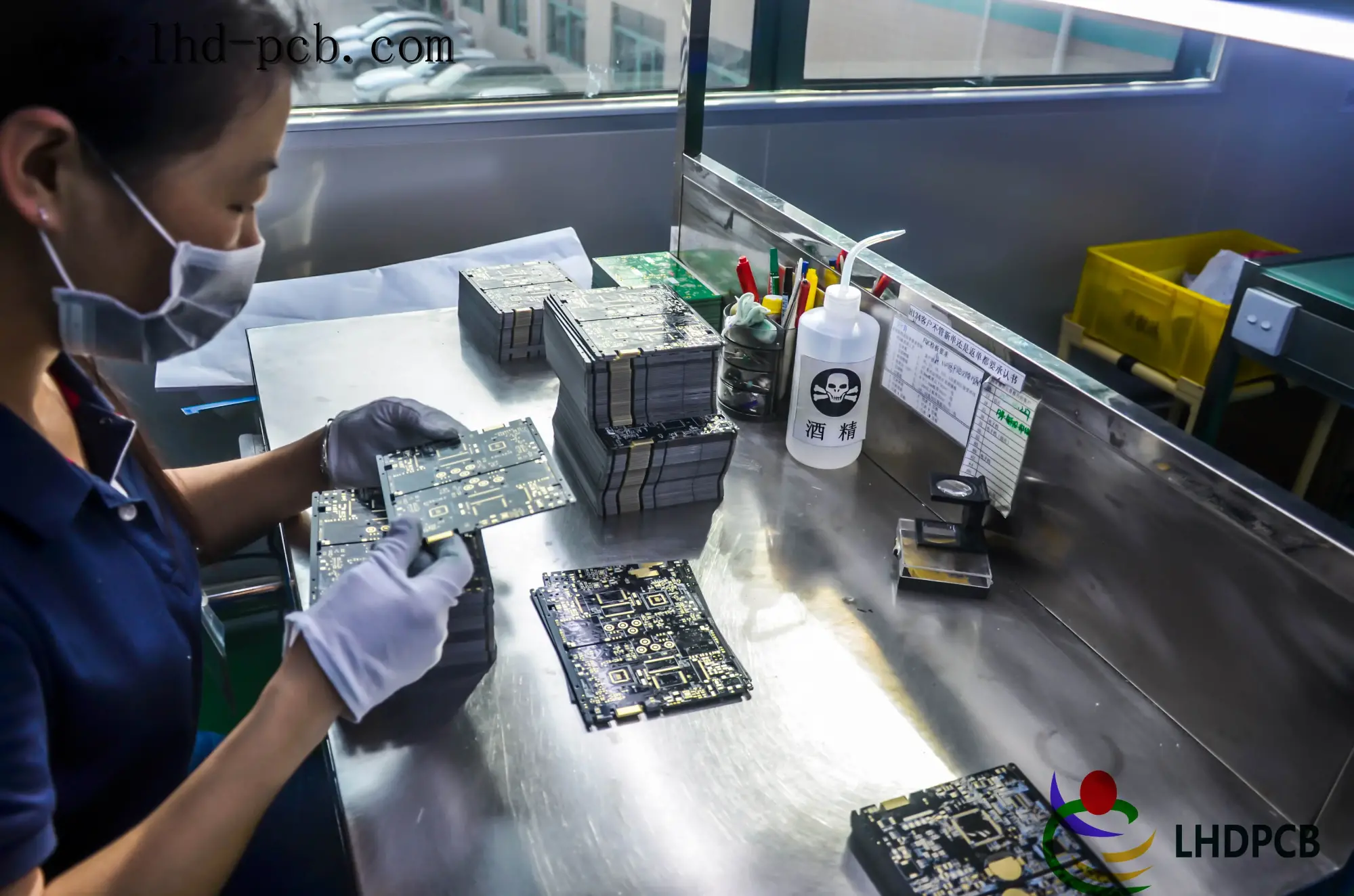
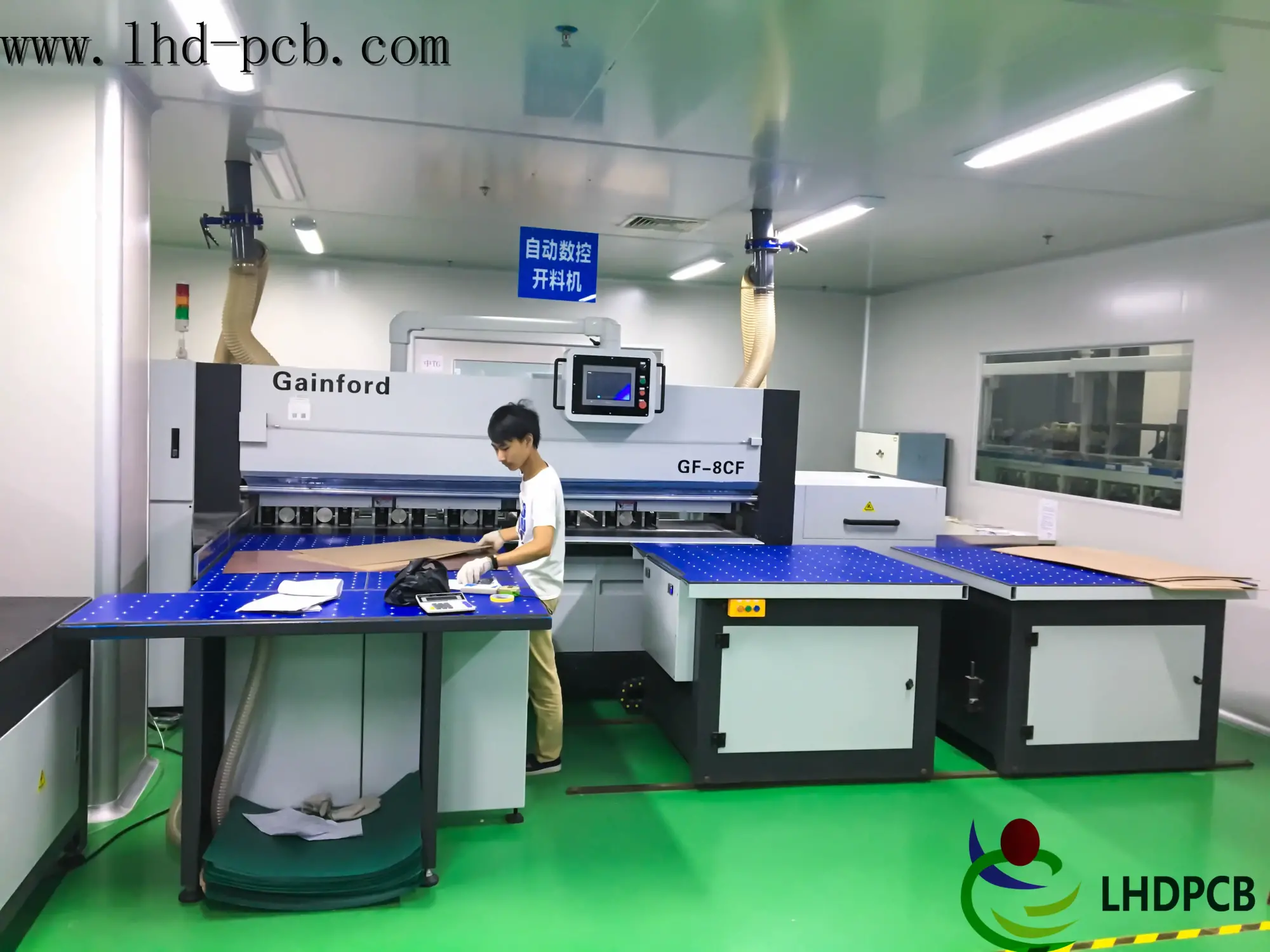
Cutting and laminating according to the size of the finished board or the size of the panel.The material need drying, the main purpose of drying is to remove the moisture in the board and prevent it from warping during processing. Generally, it is dried at 150℃ for 3-4 hours.
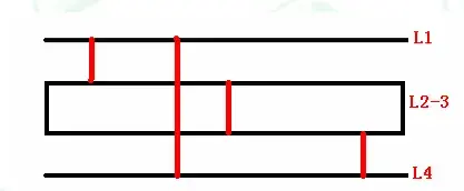
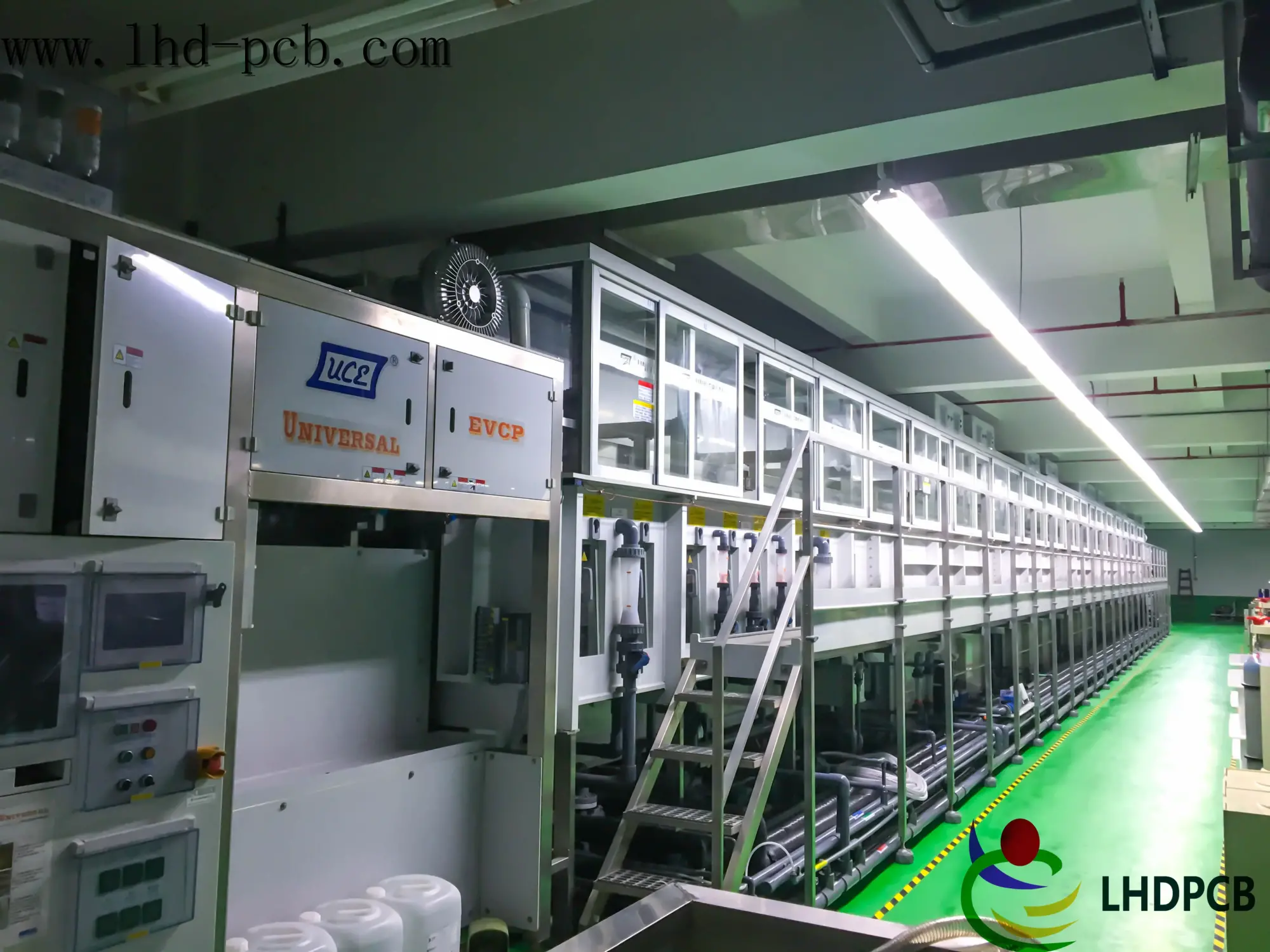
There is a process of chemical deposition of a very thin layer of copper on the hole walls before the plating process. Almost all PCB with 2 or more copper layers use plated through holes to connect the conductors between the layers. A good connection needs about 25 microns of copper on the walls of the holes. This thickness must be electroplated, but the walls of the holes are non-conductive glass cloth and resin. So the first step is to deposit a conductive layer over the hole walls. LDH tech use electrolysis copper, that is we deposit chemically a layer of copper about 1 micron thick over the walls of the hole (and incidentally across the whole panel). This is a multi-stage process as you see from the video with washing steps between the stages. LDH tech retreat the panel, then LDH tech seed the hole wall with micro-particles of palladium, and finally deposit the copper.
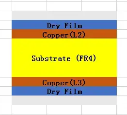
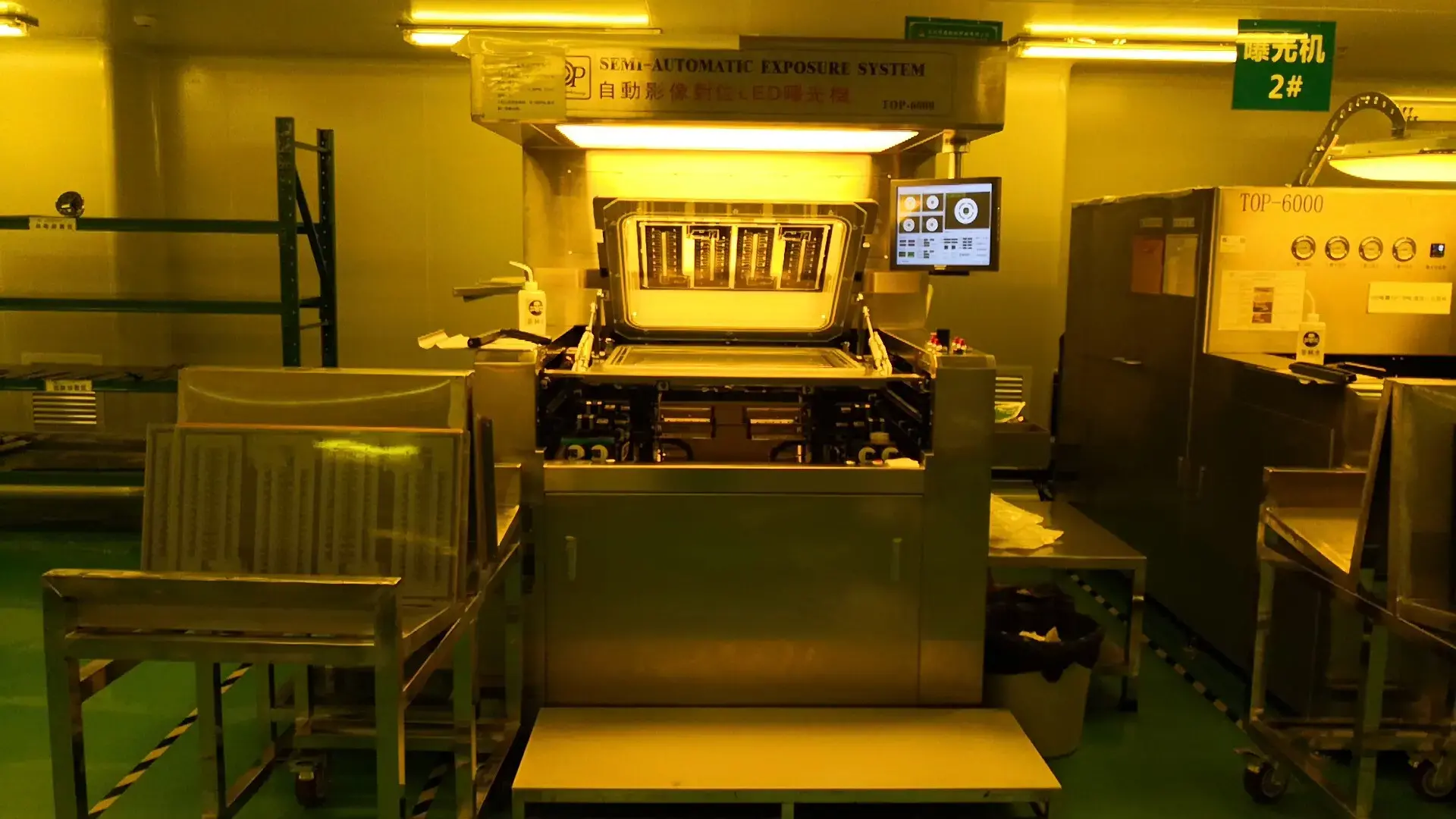
The panel is first coated with a layer of photosensitive film, the photo resist, which is hot-rolled onto the copper using a cut-sheet lamina tor. The laminated panels are collected by an automatic rack.The clean room uses yellow lighting as the photo resist is sensitive to UV light.
Next we strip off the blue photo-resist which protected the copper image. So now we have the exact pattern required. The operator checks that all the photo-resist has been removed. You can see that Euro circuits put several different designs on one production panel. That way we can make small numbers of PCB cost-effectively.
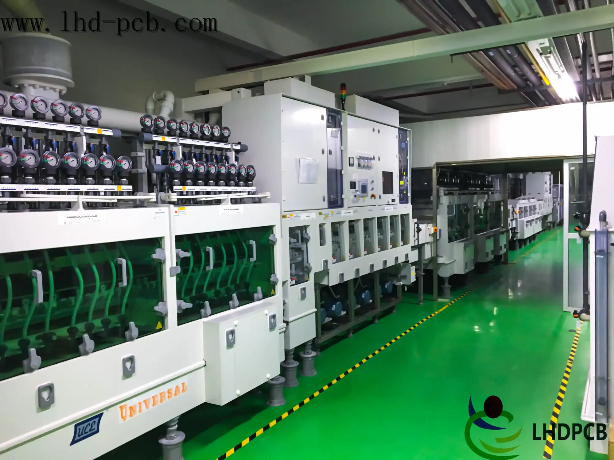
The laminating operator need placed a copper foil and 2 sheets of prep-reg on the heavy steel baseplate. Then places the retreated core carefully over the alignment pins. Then adds 2 more sheets of prep-reg, another copper foil and an aluminum press plate.
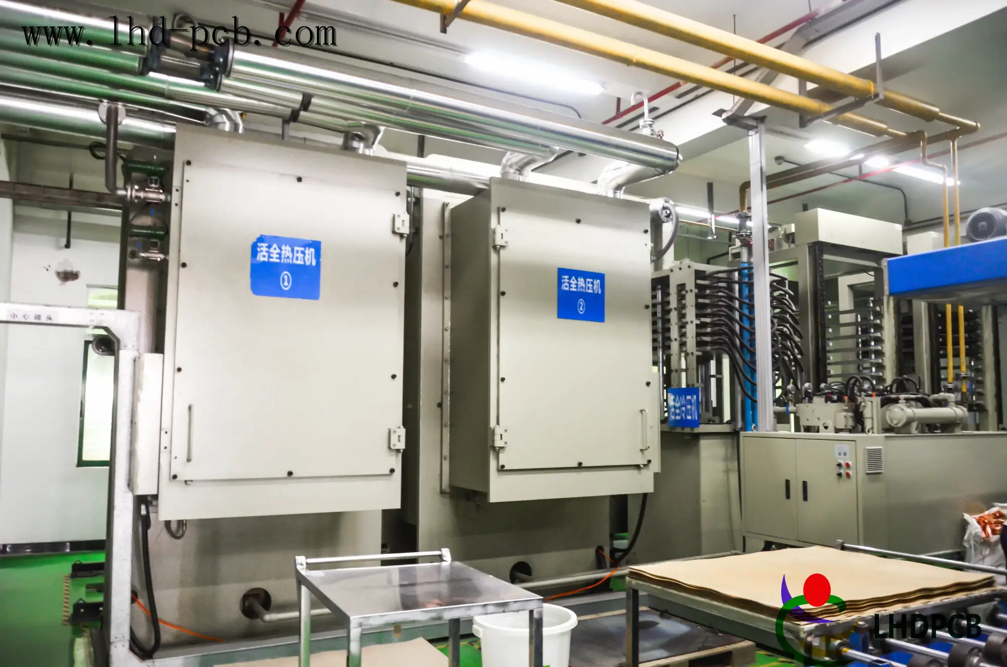
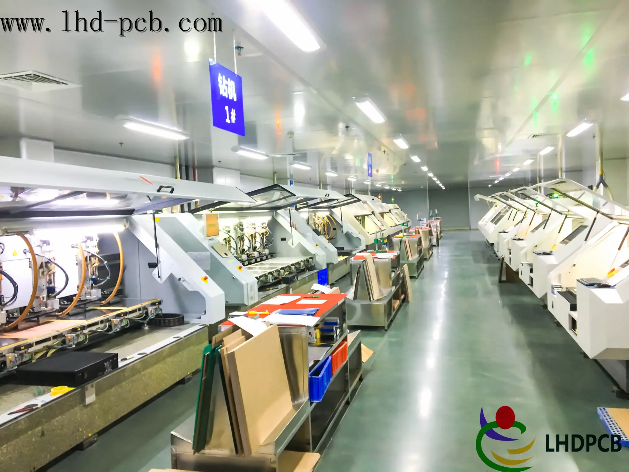
LHD tech use air-driven spindles which can rotate up to 150,000 revolutions per minute. High speed drilling ensures clean hole walls to provide a secure base for good plating on the hole walls. Drilling is a slow process as each hole must be drilled individually. So depending on the drill size we drill a stack of one to three PCB panels together. We can drill holes down to 100 microns in diameter. To give you an idea of the size, the diameter of a human hair is about 150 microns. Drill change is fully automatic. The machine selects the drill to use from the drill rack, checks that it is the correct size, and then loads it into the drill head.
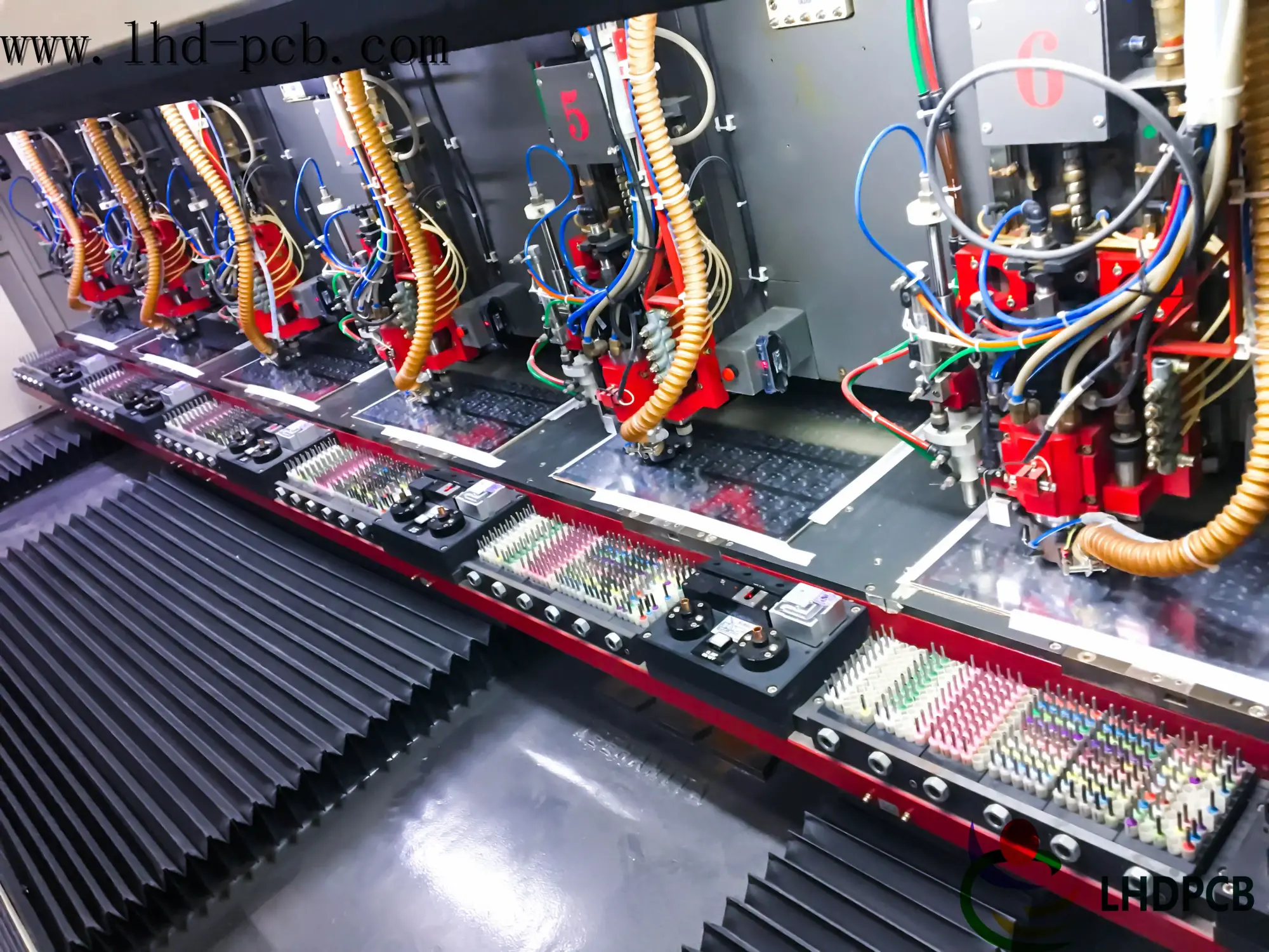
To ensure good conductivity through the holes we need to plate an average of 25 microns of copper on the hole walls. This means that we also plate 25 – 30 microns on the surface tracks. So if we start with a typical 17.5 micron copper foil it will be 40 – 42 microns after processing.
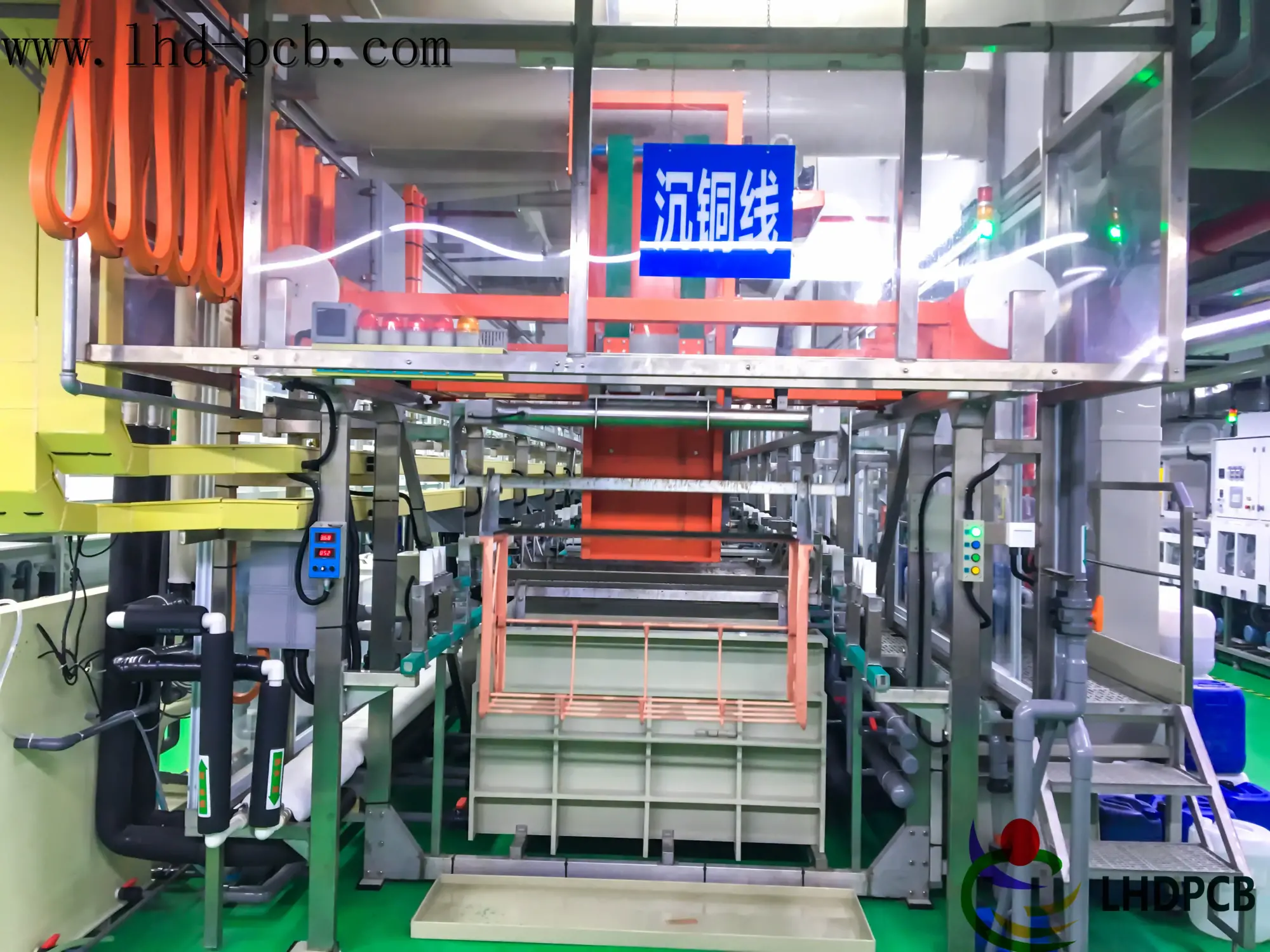
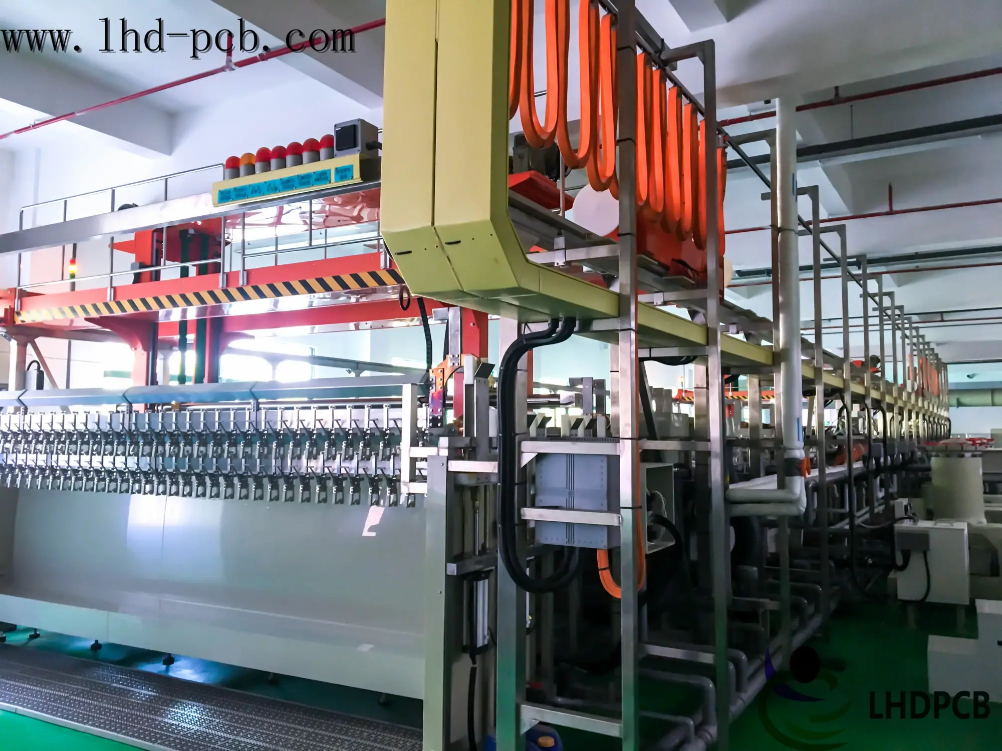
The tin used to protect the copper is removed. At this time, the copper that needs to be preserved will be exposed. Up to now, all the outer circuit patterns have been completed.
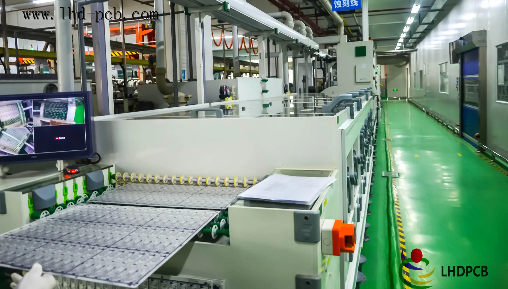
Coat the entire panel with a liquid solder mask. The board is then exposed to high-intensity UV light. Solder mask is applied to achieve the following: Protect copper circuitry from oxidation, damage, and corrosion.
LDH tech prints the solder mask under customers’ requirements and do not have an extra charge.
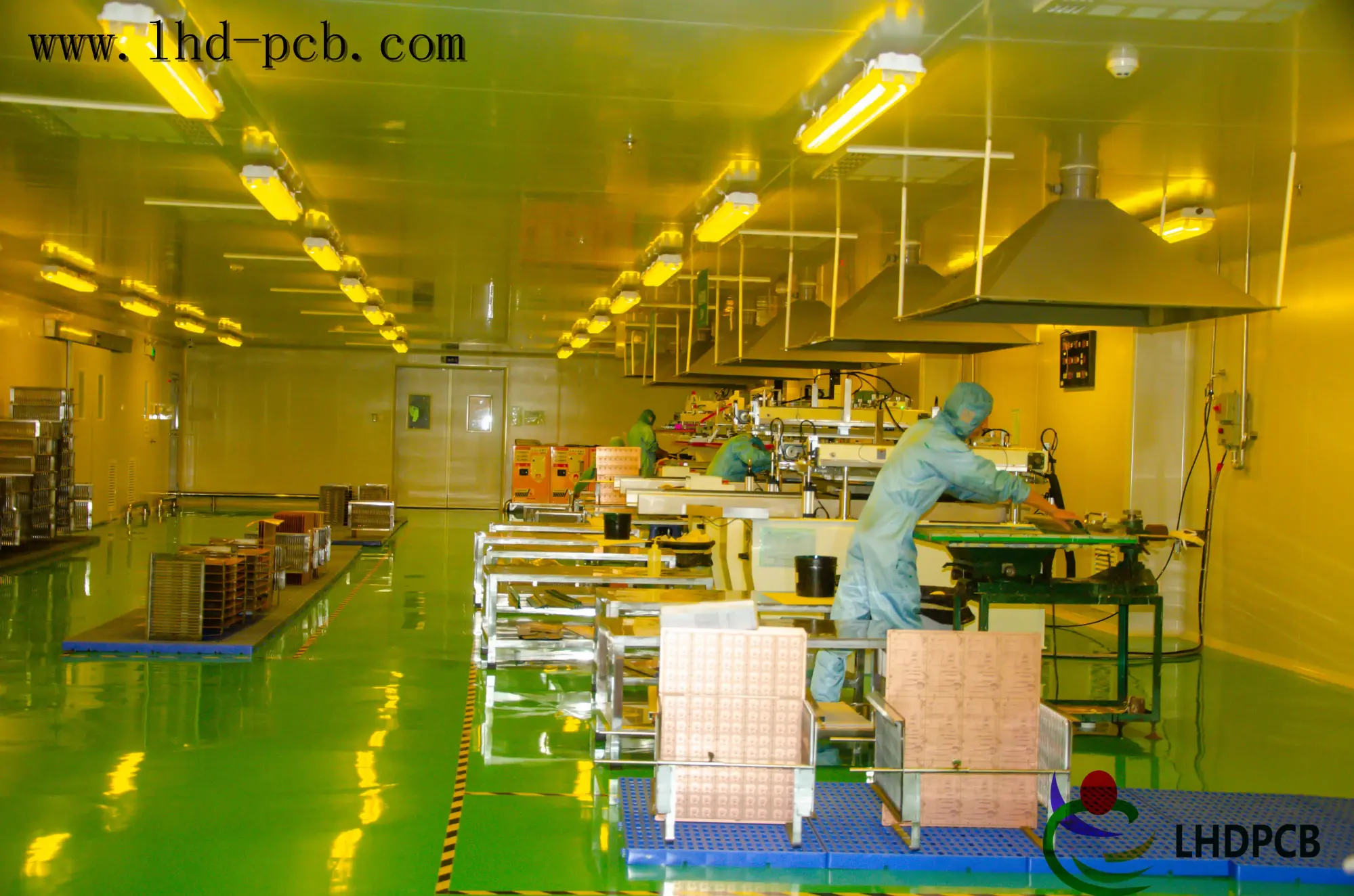
Silk screening is a vital step since this process is what prints important information onto the board. Then PCB finally passes onto the coating and surface finishing process.
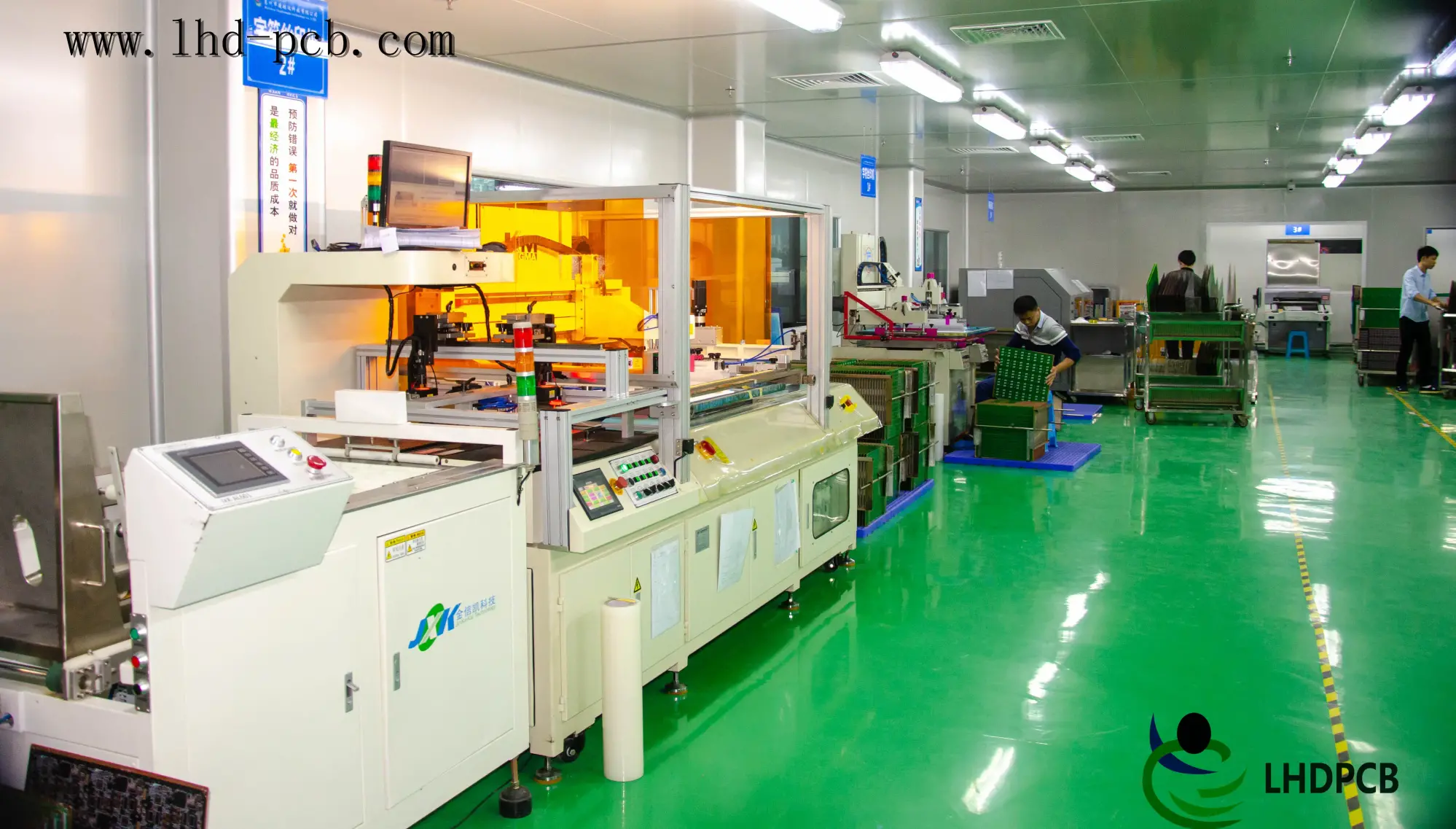
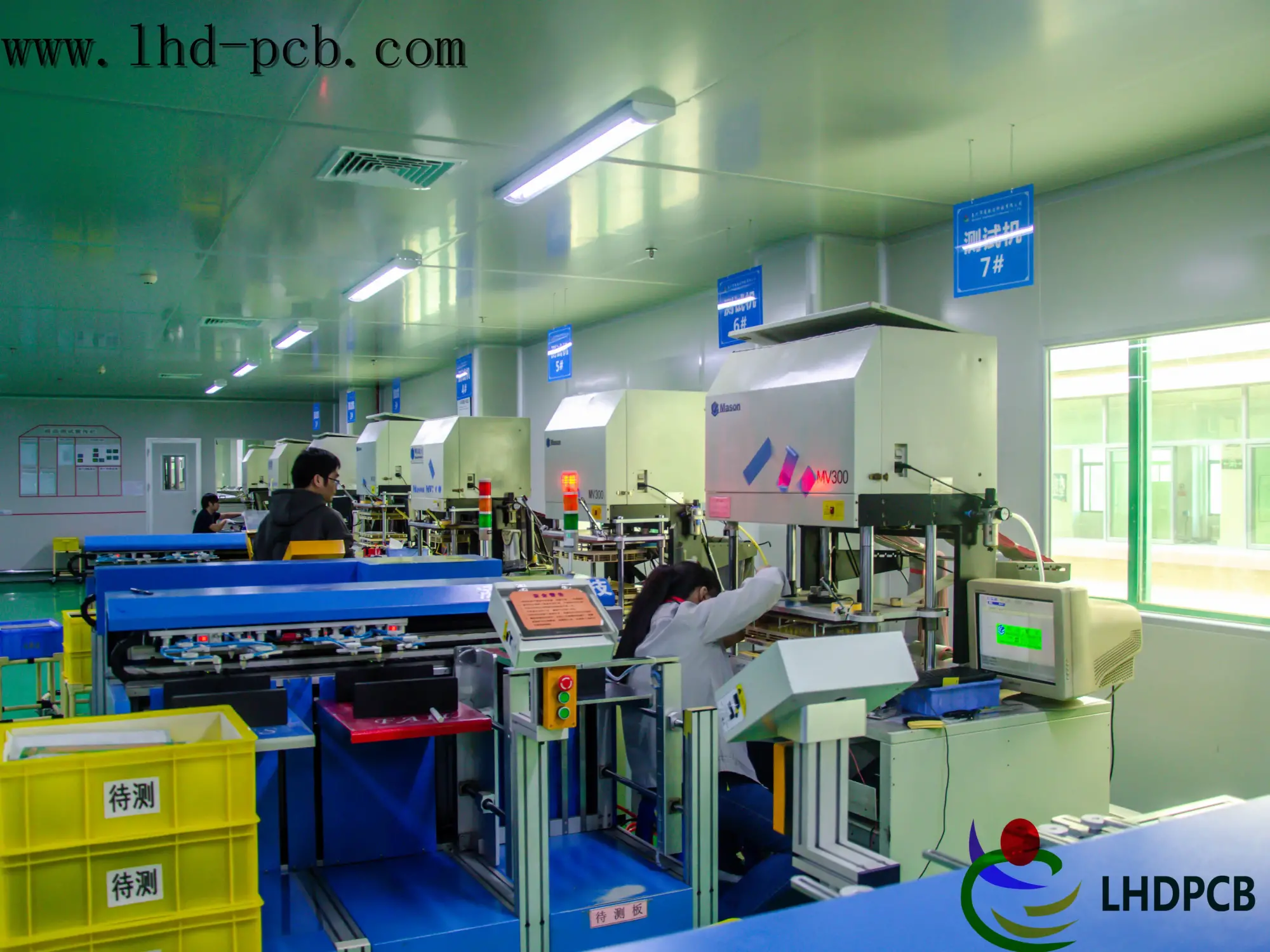
This is the final step in PCB fabrication process. The professional quality control team will perform the final inspection of each PCB. Including: visual inspection, finished product size inspection, aperture hole number measurement, war-page measurement, etc. If the inspection is qualified, we will print a test report for customer reference.
