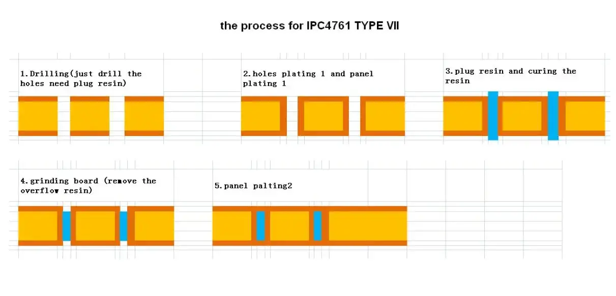
As the PCB becomes thinner and thinner and high density, many BGA placeholder areas within the PCB design is adopted the via-in-pad plated over (VIPPO) structure or called plated over filled via (POFV) structure. This VIPPO structure is better than the more traditional type pad structure, making the routing between layer and layer space wider, shortening the signal path length, reducing the capacitance, and inductance of these two parasitic effects, thus the high-speed performance is improved.
POFV is a method that resin plug vias first and then copper plating over (cladded). It also has an IPC standard, IPC4761 Type VII. Conventional technology is to separate POFV holes from non-POFV holes. Therefore, two electroplating processes are needed to ensure hole wall copper and cap&wrap plating copper thickness. In addition, in order to reduce copper thickness on the face, a thinning copper process is added after the plug holes. At the same time, in order to ensure the thickness of the cap plated copper, the reduced amount of copper can not be too large. Therefore, using the VIPPO process, often appear surface copper thickness exceeds the standard, copper thickness varies greatly, the outer etching difficult and cap copper thin and other problems, and the process is complicated, which adds difficulty to the field operation.
After many tests, data analysis, and defect analysis, different schemes for different quality defects have been formulated to verify, the research summarizes the improvement methods of each process and obtains remarkable achievements.
For more information, please contact LHD PCB.


