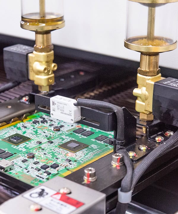
BGA PCB Assembly
Why Choose LHD Technology
01.
Advanced technology and equipment
We have advanced equipment for precise placement and soldering of BGA components, ensuring high precision and quality of assembly.
02.
Omnis Repreh
Our engineers have rich experience in BGA assembly and can provide professional technical support and solutions to ensure the successful implementation of each project.
03.
Strict quality control
We implement a strict quality management system, from raw material inspection to final product testing, to ensure high reliability and long-term stability of BGA PCB assembly.
04.
Omanis Competitive price and efficiency
By optimizing the production process and cost management, we are able to offer competitive price and faster delivery time while ensuring high quality.
BGA PCB Assembly Services
Design Evaluation and DFM Analysis
Prior to assembly, the PCB design is evaluated and DFM analyzed to ensure that the BGA components are compatible with the PCB board and that the design meets manufacturing standards.
Material Procurement
Procurement of BGA chips and other components according to the BOM (Bill of Materials).
BGA Placement
Precision placement machines are used to accurately place the BGA chips in the specified locations on the PCB.
Reflow Soldering
The BGA chips are held in place by a reflow soldering process. This process requires precise temperature control to ensure solder joint formation and reliability.
X-ray Inspection
Since the BGA solder joints are underneath the chip and not directly observable, X-ray inspection techniques are used to check the quality of the soldering.
Repair and Rework
If faulty BGA solder joints are found, repair or rework them as necessary.
Assembly Test Flow
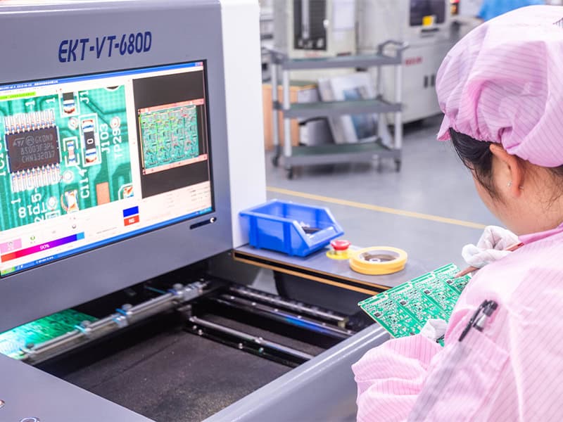
Automated Optical Inspection (AOI)
"Used to check the quality of soldering around BGA assemblies and the accuracy of component placementand accuracy of component placement."
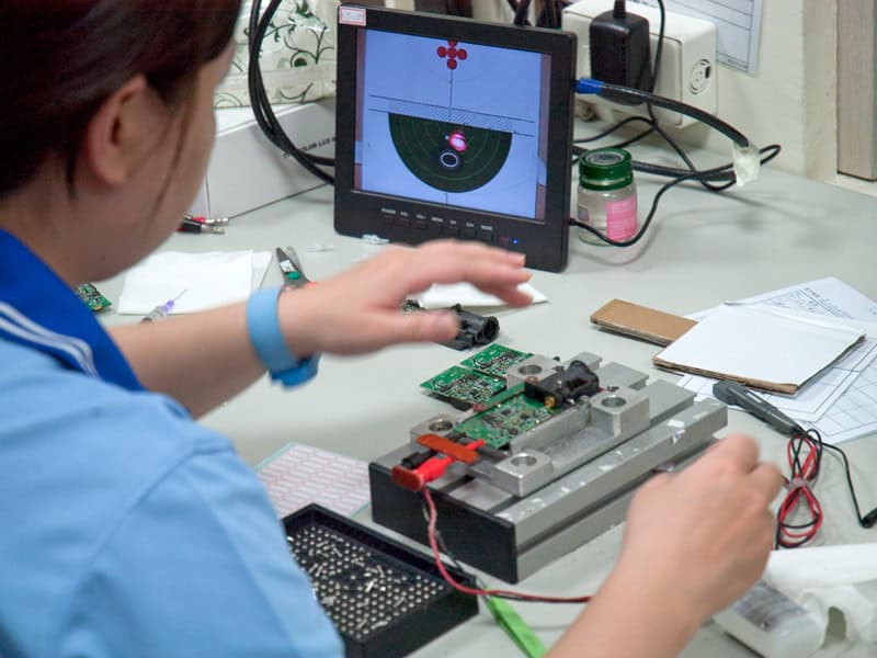
Functionality Testing
"Electrical testing is performed to verify the functionality of the PCB and to ensure that all circuits are working as designed."
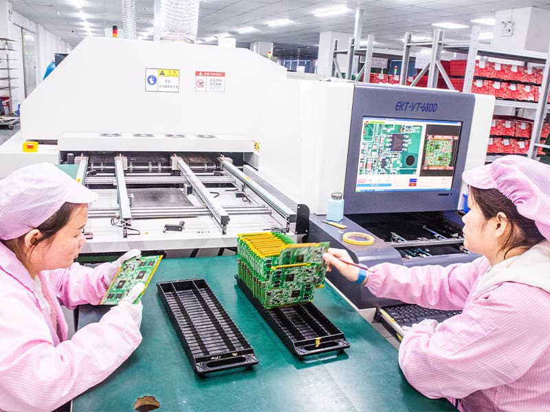
Non-Destructive Testing (NDT)
"Uses X-ray inspection or other advanced non-destructive testing methods to evaluate hidden defects under the BGA solder joints, such as the quality of the formation of spherical solder joints and possible short or broken circuits."
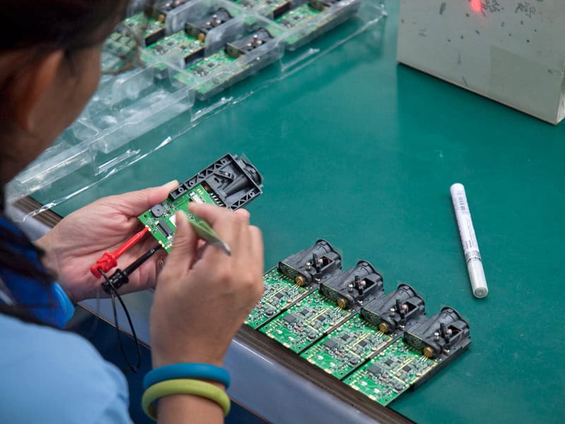
Environmental Testing
"May include temperature cycling, vibration testing, and humidity testing to evaluate the performance and reliability of the PCB under various environmental conditions."
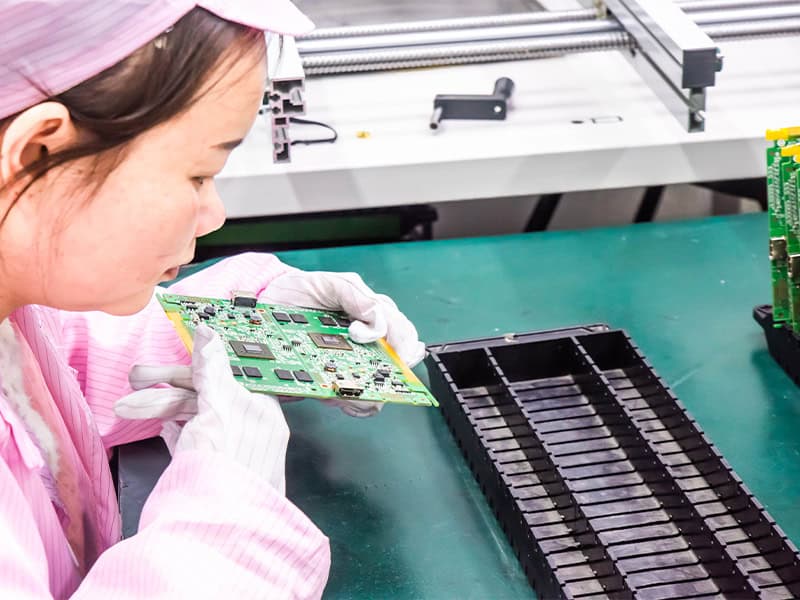
Final Visual Inspection
"A final inspection performed at the end of the entire assembly process to ensure that nothing has been missed."
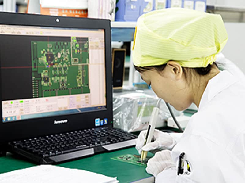
Sample Validation
"Thorough testing and validation of samples to ensure that they fully comply with design specifications before starting mass production."
Advantages of BGA PCB Assembly
High Density Connections
BGAs offer higher pin densities than traditional pin packages, allowing more connections to be realized in less space.
Better Electrical Performance
The BGA design reduces wire length, resulting in lower inductance and capacitance and improved signal integrity.
High Reliability
BGA solder joints are on the bottom of the chip and are less susceptible to thermal stress, making them more reliable than traditional pin packages.
Lower Failure Rates
The design of BGA solder joints reduces the risk of short circuits and breaks, increasing the success rate of assemblies.
Better Thermal Performance
BGA packages help conduct heat from the chip more efficiently, contributing to better overall device performance and stability.
