

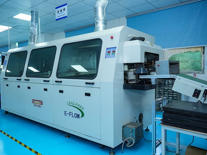
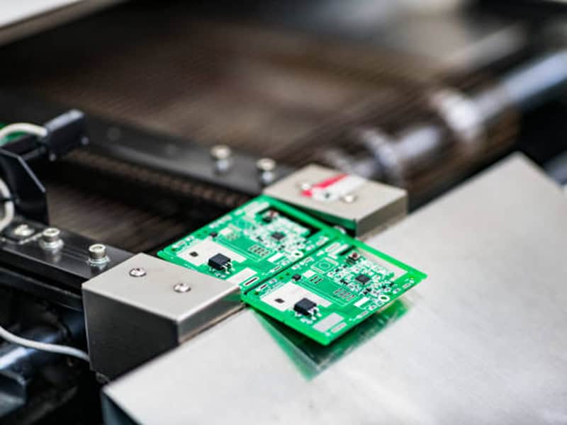
Wave Soldering
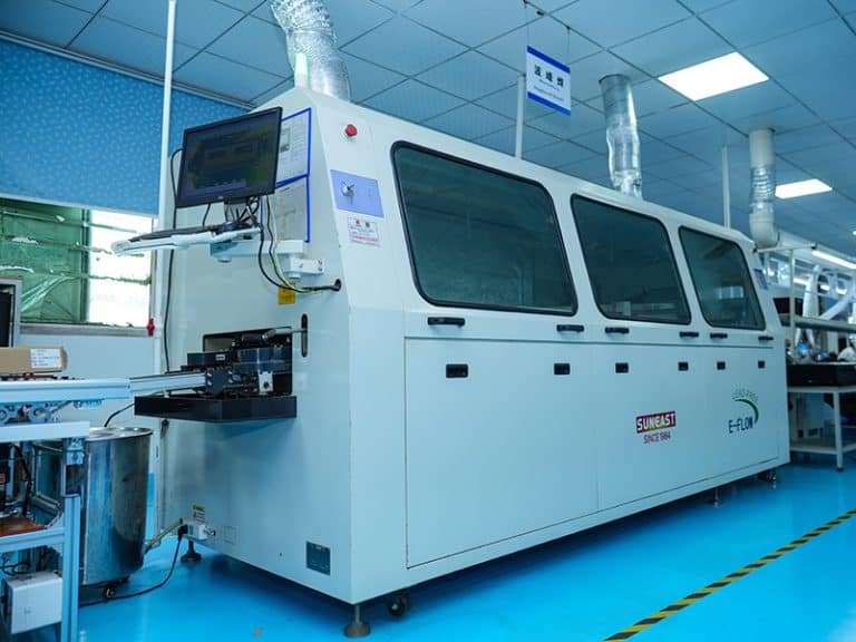
What is wave soldering?
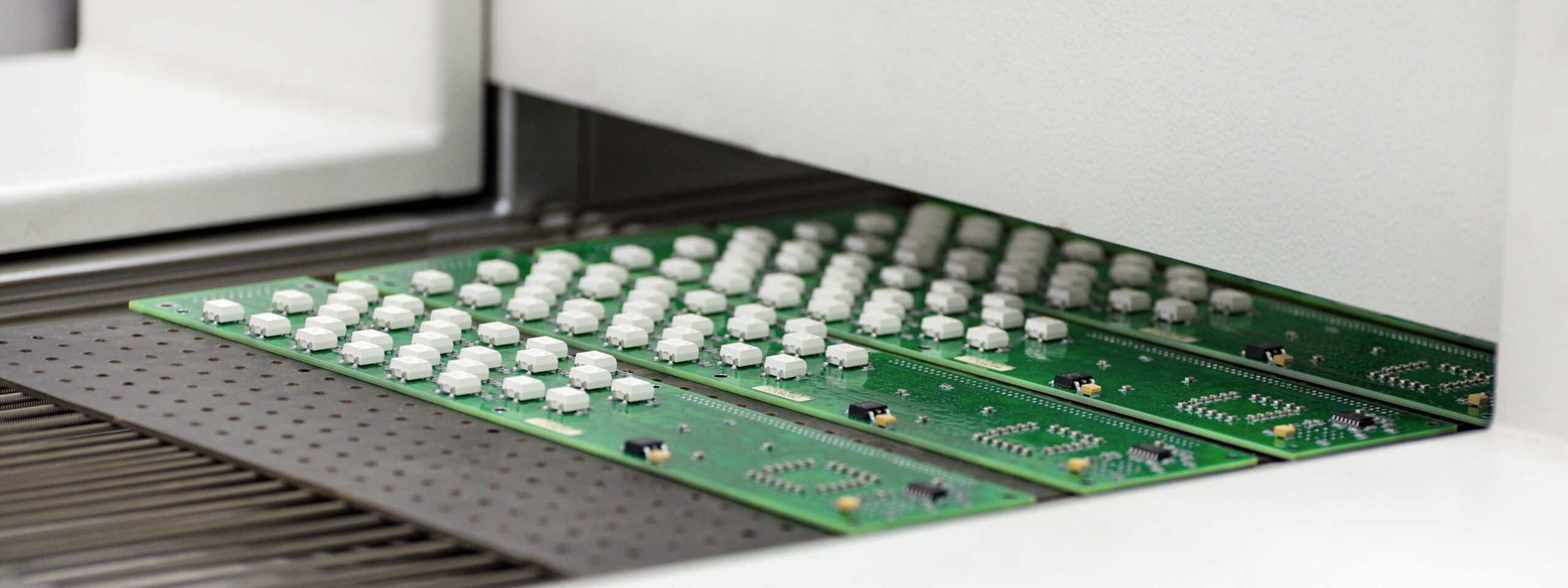
Wave Soldering Process and Defect Prevention
Wave soldering is a complex process involving multiple factors such as metal surface, molten solder, air, etc. The quality of soldering is affected by multiple factors, such as printed circuit boards, components, solder, flux, soldering temperature, time and other process parameters, as well as equipment conditions.
Therefore, to obtain an excellent soldering effect, factors such as solder formula, flux, matching of components and PCB, tooling design and process control parameters need to be considered. However, when poor soldering occurs, there may be multiple reasons. The following introduces some common wave soldering poor soldering, analysis methods of the causes and improvement suggestions.
Wave soldering process curve
The wave soldering process curve includes the following steps
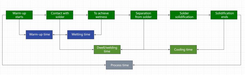
1. Wetting time
Wetting time refers to the time it takes for the solder joint to start wetting after it contacts the solder. In electronic soldering, wetting time refers to the time it takes for the solder to form a good connection after it contacts the pad. Wetting time is one of the key factors to ensure that the solder joint forms a good connection.
2. Dwell time
Dwell time refers to the time from when a solder joint on a PCB contacts the wave crest surface to when it leaves the wave crest surface. In electronic soldering, dwell time usually refers to the time the solder stays on the wave crest surface. Dwell time has an important influence on the formation and quality of solder joints.
3. Preheating temperature
Preheating temperature refers to the temperature reached before the PCB contacts the wave crest surface. In electronic soldering, preheating temperature refers to the temperature to which the PCB is preheated before entering the wave crest furnace. The purpose of preheating temperature is to reduce the thermal shock of the PCB during soldering and improve the soldering quality.
SMA type | Components | Preheating temperature |
Single-sided board assembly | Through-hole components and mixed assembly | 90~100 |
Double-sided board assembly | Through-hole components | 100~110 |
Double-sided board assembly | Mixed assembly | 100~110 |
Multi-layer board | Through-hole components | 115~125 |
Multi-layer board | Mixed assembly | 115~125 |
4. Soldering temperature
Soldering temperature is a very important soldering parameter, usually 50°C ~ 60°C higher than the melting point of solder (183°C). In most cases, it refers to the temperature of the soldering furnace. In actual operation, the temperature of the soldered PCB solder joints should be lower than the furnace temperature, because the PCB absorbs heat. The soldering temperature has a decisive influence on the formation and quality of the solder joints. The appropriate soldering temperature can ensure that the solder joints are firm, the quality is stable, and reduce soldering defects.
Wave soldering process parameters
• Wave crest height:
The wave crest height refers to the height of the tinned PCB during wave soldering. This value is usually controlled between 1/2 and 2/3 of the thickness of the PCB. If it is too large, it may cause the molten solder to flow to the surface of the PCB and form a "bridge".
Wave soldering process parameters include the following
• Conveyor inclination:
When installing the wave soldering machine, in addition to making the machine level, you should also pay attention to adjusting the inclination of the conveyor. By adjusting the inclination, you can control the soldering time between the PCB and the wave soldering surface. The appropriate inclination helps the solder liquid to peel off the PCB faster and return it to the tin pot.
• Hot air knife:
The so-called hot air knife is a narrow and long "cavity" with an opening placed under the SMA just after the SMA leaves the welding wave crest. The narrow and long cavity can blow out hot air flow, like a knife, so it is called a "hot air knife".
• Solder purity:
During the wave soldering process, impurities in the solder mainly come from copper leaching from the pads on the PCB. Excessive copper will lead to increased soldering defects.
• Flux:
Flux is a chemical used in the soldering process that helps remove oxides and improves solder wetting and fluidity. In wave soldering, using a suitable flux can improve soldering quality.
• Process parameters:
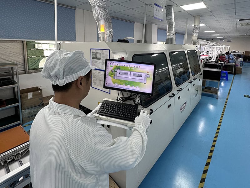
The process parameters of wave soldering machines include belt speed, preheating time, soldering time and inclination angle, etc. These parameters need to be coordinated and adjusted with each other. Belt speed and preheating time will affect the soldering quality and the reliability of solder joints. Soldering time and inclination angle will affect the contact time between solder liquid and PCB and the formation quality of solder joints. Therefore, these parameters need to be adjusted repeatedly to obtain the best soldering effect.
Wave Soldering Defect Analysis
How to deal with wave soldering defects
Wave soldering is the process of heating the soldering liquid to produce molten liquid solder, and connecting the joints on the electrical circuit board with the components already soldered on the circuit board through the flowing liquid solder.
1. Cold welding
The welding point is not full and the solder fluidity is poor. The reason for cold welding may be too many impurities in the solder or the welding temperature is not enough.
Solution:
For cold welding, you can adjust the welding temperature so that it is within the appropriate range. At the same time, regularly check the quality of the solder to avoid excessive impurities.
2. Bridging
Two adjacent solder joints are connected, resulting in a short circuit.
Solution:
For bridging, the circuit board design and component layout can be optimized to avoid connecting adjacent solder joints.
3. Bubbles
During the welding process, bubbles are generated due to high temperature, which prevents the solder from fully filling the solder joints, affecting the welding quality.
Solution:
For bubbles, you can adjust the welding time and welding pressure to make the solder fully fill the solder joint.
4. Cold soldering
The solder joint was not fully fused, resulting in poor contact.
Solution:
For cold solder joints, the fusion degree of solder joints can be ensured by improving the quality and cleanliness of solder joints.
5. Offset
During the welding process, the position of components shifts, causing circuit short circuit or open circuit.
Solution:
For offset, the correct position of components can be ensured by optimizing the welding process and component fixing method.
In short, during the wave soldering process, the quality of the solder and the status of the soldering equipment should be checked regularly to promptly detect and resolve soldering defects and ensure soldering quality and electrical performance. At the same time, quality inspection and quality control should be strengthened to ensure that each soldering link meets standard requirements.
